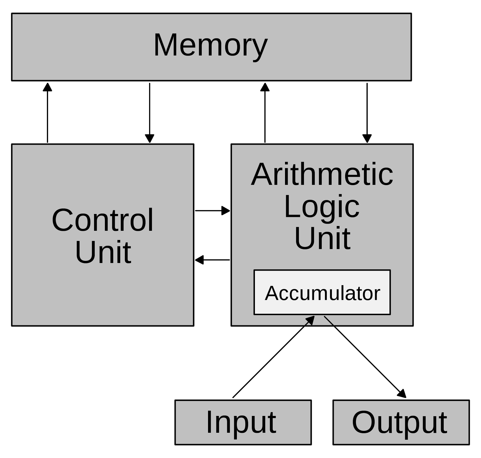
Von Neumann Architecture


ALU: Arithmetic Logic Unit Accumulator: Does addition
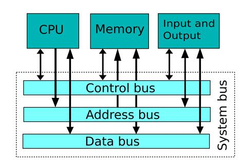
Buses
Address Bus: Transmits the address from the processor to the memory or I/O controller. Unidirectional: from the processor to memory and input-output devices.
Data Bus: Sends data between the processor, memory and input-output devices. It is bidirectional.
Control bus: Signals sent by the processor to control the memory and peripheral devices. Bidirectional: From the processor to the memory and input-output devices.

Address Bus
- Memory is divided into several fixed segments called words.
- The words may be sized at 16,32 or 64 bits, depending on the processor.
- The addresses of operands are sent via the address bus.
- The results are calculated by the processor and stored in a particular memory location, the address of this is transmitted via address bus.
Data Bus
- A bidirectional bus consisting of 8,16,32,64 parallel lines.
- Transmits instructions and data between the processor and the, memory and I/O devices.
Control Bus
- A bidirectional bus that transmits timing, status signals and commands between the processor, memory and I/O devices.
- Makes sure that data is travelling to the correct place at the correct time.
- Different control signals are:
- Clock: Synchronise the operations of the computer.
- Memory Read: The contents in the specified address are copied to the data bus.
- Memory Write: The contents of the bus data bus are copied to the specified address.
Registers
- Program Counters: Holds the address of the next instruction to execute.
- Current Instruction Register: Holds the current instruction being executed.
- Memory Address Register: Holds the data address of the register from which data is read, or to which data is to be written.
- Memory or Data Register: Temporarily stores the data being read from or written to the memory.
- Status Register: Holds the bits that are set or cleared based on the results of an instruction.
Stored program concept: Machine code instructions stored in main memory are fetched and executed serially.
General purpose registers are named R0-R12
Memory Unit
- A memory unit consists of a number of partitions
- Each partition consists of data and and address
Read Operation
- To read the contents from any location, the registers MAR (memory address register) and MDR (memory data register) are used.
- A read signal is sent by the processor to the memory. The contents are then copied to the MDR.
Write Operation
- To write data into a particular address, the data is first written to the MDR.
- The address is then written to the MAR.
- A write signal is sent by the processor to the memory unit through the control bus and the location is written to with the data in the MDR.
Processor ALU & CU
- The processor contains ALU (Arithmetic Logic Unit) and CU (Control Unit).
- The ALU is responsible for arithmetic functions such as addition, subtraction, multiplication etc and logic operations such as AND, OR, NOT etc.
- The Accumulator (ACC) is the register that stores the result of arithmetic and logical operations performed by a processor.
Processor: CU
- The control unit (CU) is responsible for controlling the memory, processor and input-output devices.
- It contains the CIR (Current Instruction Register) and PC (Program Counter).
- The CIR contains the current instruction carried out by the processor.
- The PC contains the location of the instruction that is to be executed next.
- The control unit reads the instruction from the memory, decodes it and sends control signals to the memory and I/O devices.
I/O Controller
-
Each device has its own controller which is connected to a control bus. I/O controller is responsible for receiving the requests from the processor and sending control signals to the device specified for that operation.
-
it consists of:
- An interface to connect it to the system or I/O bus.
- a set of data, command and status registers/
- an interface
Assembly Language
-
Assembly is a low level programming language equivalent to machine code or binary instructions on a 1:1 basis.
-
It uses some word like structures to represent the instructions given to the CPU.
-
Mainly used in embedded systems because it is time consuming specialist work.
-
Assemblers translate it into machine code.
-
Different CPUs have different different machine and assembly codes.
-
Assembly operations are split into an opcode and an operand—LDR 2A
-
Opcodes are instructions. Ie, LDR = Load
-
Operands are locations or data values. Ie, 2A = 42 in Hexadecimal
Assembly Language Addressing
Immediate addressing:
- The operand is the data
- LDR R1, #42 = Load 42 into register 1
- Hash specifies a decimal value
Direct addressing:
- The operand is the address of the data
- LDR R0, 103 = Load the data at memory address 103 to register 0
- This can be a main memory address or one of the registers
Other forms of addressing do exist, but are not relevant for A Level.
Assembly instructions are provided in an exam, you do not need to learn them.
RISC vs CISC
RISC:
- complex instruction set processors have more and more of the commands at assembly level
- they can interpret high level languages more directly
- they run complex algorithms more effectively
- this leads to more complex chip designs and higher energy use but simpler code conversion
CISC:
- reduced instruction set processors can’t directly translate the high level instructions
- this leads to more lines of code at the assembly level
- they are more simply designed processors and run simple commands faster
- RISC processors can use pipelining, simple commands can be run simultaneously
Control Bus Signals
- The different control signals transmitted by the control bus are:
- Clock: Synchronise operations of the computer
- Memory Read: The contents in the specified address is copied to the data bus
- Memory Write: The contents of the data bus is copied to the specified address
- Bus Request: A device requests to use the data bus, so it can perform a read/write operation
- Bus Grant: Signal from the processor indicating that the device is granted access to use the data bus.
- Interrupt Request: An interrupt is a signal sent by a device requesting access to the processor.
CBS questions
a) 9D needs reading.
- Increment PC
- MAR 9D
- Bus request sent to request a read operation.
- Control Unit approves read operation.
- Bus Grant returned to authorize bus usage.
- Memory Read performed to copy the contents of address 9D into the data bus.
- Data saved to the MDR (memory data register)
b) To write the data 76 to address 99, you would need to:
- Increment PC
- Bus request for write operation
- Control Unit approves write operation.
- Bus Grant returned to approve write operation
- Memory Write to store the literal #76 in the address 99
- Data bus moves data to address and saves it
Fetch-Decode-Execute cycle
Fetch
- The program counter contains the location of the instruction that is to be executed next. This address is copied to the MAR.
- The instruction is fetched from the memory and copied to the MDR.
- Then the contents of the MDR is copied into the CIR.
- The value in the PC is incremented by 1 and the instruction in the next memory location is processed.
Decode
- The instructions are decoded so that it can be executed.
Execute
- The processor sends appropriate control signals to the memory unit and input-output devices in the computer system according to the decoded instruction.
Registers (RECAP)
PC: Program counter contains the allocation of the instruction which has to be fetched. MAR: Using the address bus, the contents of the PC is copied to the MAR MDR: The instruction at that particular location is copied to the MDR temporarily CIR: Stores the currently processing instruction
Interrupts
- Interrupts allow the computer to carry out many tasks at the same time
- When the interrupt is serviced, the status of the current job is saved. The contents of registers PC and CIR are saved onto the system stack.
- Once the interrupt is serviced using the interrupt service routine, the current job is serviced according to its status when it was saved before the interrupt service.
Vectored Interrupt Mechanism
- Each interrupt is associated with a vector, which points to the code associated with that interrupt
- When an interrupt occurs, the current values of the registers are saved to a stack memory structure and the processor identifies the type of interrupt.
- Then the processor points to the vector and processes the interrupt service routine. This technique is called vectored interrupt mechanism.
Interrupted Interrupt
- Sometimes, when an interrupt is being serviced, another interrupt occurs.
- The processor may save the status of the current interrupt processing and proceed to service the new interrupt.
- Another methodology that can be used is priorities. In this methodology, we prioritise the most important interrupts first.
End of Topic
-
What are the three types of bus and their functions? Data bus → Transports data between components Control bus → Carries control signals and instructions Address bus → Allows referencing of memory locations
-
How are memory locations addressed? Each memory location has a unique ID which allows for it to be referenced through a memory address bus.
-
The ALU is responsible for various arithmetic and logical functions within the processor.
-
The control unit controls the memory and peripheral devices through control signals sent over the control bus (lots of control). It also receives interrupts over the bus.
-
List different registers
- CIR - Current Instruction Register
- PC - Program Counter
- MBR - Memory Buffer Register
- MDR - Memory Data Register
- MAR - Memory Address Register
- SR - Status Register
- ACC - Accumulator
Processing Speed
- Depends on the speed of the CPU, memory and bus speed.
CPU Performance
- Four impacting factors are:
- Cores
- Clock rate
- Cache size
- Processor type
Cores
- A CPU consists of multiple processing units. Each processing unit is known as a core.
- A core consists of a processor (ALU and CU) and registers.
- Computers may be dual, quad or higher core counts.
- As the number of cores increases, the computer has more power to execute multiple programs at once.
Cores Linked
- As more cores are used, communication channels between cores increase exponentially.
- These communication channels drain some performance from each core, as every core must communicate with every other core.
Clock Rate
- Clock rate indicates the number of instructions processed by a CPU in a second.
- It is measured in megahertz (MHz) or gigahertz (GHz)
- A 4GHz processor handles around 4 billion instructions a second
- A faster CPU requires more power and produces more heat
Overclocking
- The speed of a computer can be overridden by the BIOS,
- Increasing the clock speed of your CPU is called over-clocking
- There are circuitry limitations regarding the speed. If a computer is forced to work at a higher speed, more than its limit, the instructions might not get executed completely. This leads to data corruption and overheating.
Cache
-
Cache is a small memory part located closer to CPU when compared to RAM
-
Cache temporarirly holds the data and instructions that the CPU is likely to use more frequently
-
To reduce the access time, the control unit checks cache first before requesting any instructions from RAM or main memory.
-
Cache is located directly on the CPU chip.
-
Due to the presence of cache, the speed of CPU increases.
Cache Types
Level 1:
- 8KB to 64KB
- On the CPU chip
- Fastest access time
- Smallest cache in the CPU Level 2:
- Bigger than L1
- Between CPU and RAM
- Slightly slower than L1 Level 3:
- Further from the CPU but still closer than the RAM
- More storage than L2 cache
L1 and L2 cache are dedicated to each core, however L3 cache is shared between all cores.
Cache Size
- It is important to note that cache occupies only a small space compared to RAM
- Cache is also expensive when compared to RAM.
- L3 cache is typically around 4MB
Data Word Size
- Each word has its own specific address
- In case of read and write operation it is important for us to know the address of the memory location.
- The larger the data word size, the more RAM you can use, the more operations you can handle at once, the larger the number of available opcodes on the instruction set etc
- Typical sizes: 32-bit,64-bit,128-bit
Embedded Systems
- Programmed during manufacturing stage
- Users operate these using interfaces such as buttons or touch screens
- The software cannot be modified, it is typically bult into the physical chip
Input devices
2D Scanners
- Read head moves over the page, detects light and converts dark and light patches into a digital image.
3D Scanners
- Similar to a 2D scanner, but also using lasers and building a three dimensional model of the object—creating an asset that can be used in games, movies or any other purpose.
Barcode Reader
- Read by a laser
- Light reflected back into the sensor
- Light and dark areas can be distinguished
- This is then used to distinguish between different products and communicate what product is being purchased to a PoS system.
QR Codes
- A binary pattern encoded into an image
- QR Codes are up to 7000 digits whereas normal barcodes can only store 30 digits
- With Internet access, QR codes can be scanned anywhere.
- They are widely used for advertising products on public transport in public areas.
Digital Cameras
- Microprocessor automatically adjusts shutter speeds, focus the image, operate the flash, adjust the aperture etc etc
Microphone, Keyboard and Mouse
- Not noted, basic.
Voice Recognition System
-
Used in security systems
-
It has software to compare the wave pattern of the sound from the user to the wave pattern stored in its memory.
-
If the two wave patterns match, then the user is identifies.
-
Breaks different sounds into phonemes.
Radio Frequency Identification (RFID)
- A technology to identify and track tags attached to items such as cars, animals, bank cards etc
- Identified using electromagnetic fields without a line of sight
- Consists of a transponder and an antenna
Passive tags
- Powered by the energy from the RFID reader’s radio waves.
- Cheaper compared to active tags
- Used when reader is less than one meter away
Active tags
- Powered by batteries and can send signals at a greater distance from the reader.
- Used for tracking catds etc
Sensors
- Read physical information and produce a digital output that cna be used by a computer
Output
Inkjet Printer
- Sprays ink onto a page to convert a digital file to a physical document.
Piezoelectric
- A crystal at the back of the ink reservoir is given an electric charge and a vibration is created.
- This vibration forces the ink to be ejected onto the paper.
Thermal Bubble
- Tiny resistors produce localised heat that vaporises ink.
Laser Printer
- Uses powder instead of ink.
- Uses static electricity to print.
- Prints the whole page in one go.
- Carries large print jobs out at higher speeds than inkjet.
3D Printers
- Layer plastics on a base in a specific way to result in a model being produced.